Wednesday, April 27, 2011

Operational Amplifiers

The idea behind the op amps lab is to apply operational amplifiers in a real world scenario. There may be many instances in the real world where a circuit may be required to have a different set of voltages at different parts of it. For example, a sensor which captures certain information may not be outputting an ideal voltage for it to work with the attached processing unit. Enter the Op Amp which can make it work! The following circuit was built and all the values were recorded.


Once the circuit was constructed, it was apparent that the circuit contains a feedback loop. By putting a resistor in between the output voltage and the input voltage, the operation amplifier can be made to output the desired voltage gain.

The circuit was then connected to two separate voltage sources providing various voltages starting from 0 and ending in 1. We went in 0.25 volt increments. The following is


Vin Vout GAIN Vri Iri Vrf
0 0 0 0 0 0
0.25 -2.39 9.958 0.24 0.235 2.39
0.5 -4.9 9.8 0.5 0.504 4.9
0.75 -7.44 9.92 0.75 0.707 7.43
1 -9.93 9.83 1.01 1 9.93


It came out that the current being drawn from sources were about 7.5 and 1.8 milliamps. These were not expected but that may be in part due to the fact that the power supplies (voltage supplies) were also being used to power the voltage dividers.


Sunday, April 3, 2011

PSPICE Webassign Homework

The latest Webassign homework assignment was designed as further practice in utlilizing PSPICE to solve circuit problems. The two problems were worked out by hand first and the answers were then compared to PSPICE analysis results. The first problem was as follows;


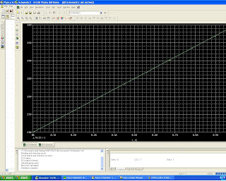
In order to solve the problem. The circuit was first constructed in PSPICE schematic with the exception of the Load being replaced with a probing current source. The idea is to run a sweep across the load with various currents (0-1 mA) with 0.1 mA increments. The results were then plotted. Here is a screenshot;


In this case, the 0-intercept (where the resistance across the load is infinite which is why the current is 0) is the Thevinin voltage while the slope of the line (voltage/current or V/I) is the Thevinin Resistance. The second problem also incorporated calculations for the maximum power displacement across the resistor. The question is as follows.


The first part of the problem was solved in the same method described for problem one. The second part of the problem involved using an actual sweeping resistance across the Resistor. The following screenshot shows the graph along with the circuit constructed in PSPICE Schematic.

With various theoretical resistances across the load, the resulting power dissipation graph was plotted so as to determine the optimum power dissipation.

Overall the results were very close to the calculated values (well within 5% which can be attributed to rounding errors). PSPICE demonstrates that there is a way with the computational power of a PC to calculate values across a circuit by setting a varying source or load and then plotting the results. The graph can then be analyzed and used to find the appropriate values. However, the PSPICE graph also gives the engineer and idea of how the circuit would operate across multiple conditions and save the engineer a lot of tedious calculations and time!

Friday, April 1, 2011

PSPICE Lab #2

The second PSPICE lab is designed to test some applications of the P SPICE engineering simulation software. The first lab was more to familiarize people with the Graphical User Interface of the program. One of the core concepts to take away from the PSPICE LAB #2 is that the program is intended to provide engineers with a quick way to design and test various designs. It would be impractical to build a prototype for every single theory or design and so P SPICE is used as an intermediate in order to separate the designs that are theoretically sound enough for Prototypes.


The Circuit on the right was created in PSPICE Schematics and involved use Viewpoints which are a neat tool to set PSPICE to display any electrical information at a point on the circuit designated by the user.


The Graph on the Right is an example of the type of graphing capabilities possible with the software. A varying voltage source which varies between 1-20 Volts at 1 Volt Increments is used as an example.

For more complex analysis involving dependent sources like the circuit on the left.

The following graph maps various factors and values.


Consequently, to figure the Norton Current, a probing voltage source is put in place of the load. The idea is to set an artificial voltage across the load and figure out the current across that voltage source.


The circuit on the left here is meant to be the thevinin representation of a more complex circuit. PSPICE can also calculate a variety of different capabilities of a given circuit including the maximum power dissipation when facing a varying load capacity.


The following power graph is a trace of the values of the power dissipated across the load at various resistance levels.


PSPICE's ability to quickly analyze a circuit with sweeping loads and source values is a valuable tool for the electrical engineer. Not only does it provide a quick way to calculate Norton and Thevinin values, it is also a way of calculating the values across a circuit under various conditions. Analysis of these graphs provide engineers with a way of seeing the best ways to implement a circuit design.

Thevinin Equivalent Lab

The Thevinin lab is designed to familiarize participants with the real life applications of Thevenin's theorem. In reality, circuits are not as simple as the ones shown for practice problems in electronic engineering classes. Thevinin's theorem allowed for every circuit no matter how complicated to be essentially be broken down into a single voltage source in series with a resistor.


The picture above shows the circuit as it was set up to be just a Thevenin equivalent circuit. Measurements were then taken.


CONFIG THEO VALUE MEASURED % Error
RL2=RL2,min 8 7.68 4%
RL2=Infinite 8 8.50 8%


Overall, the percent error for the following lab was a little higher than usual. This was due to various factors such as resistors being off by +/-5%. The most expensive thing in engineering is precision and since most commercial ventures do not have an unlimited budget to purchase near perfect parts, most will try to limit error percentages by building more efficient circuits. One observation made from this lab is that reducing error in a circuit can sometimes mean using more resistors in parallel and series to minimize error by spreading it out among multiple components instead of gambling on one.